NVIDIA NVHBM and NVLink Fusion: Custom HBM Base Die for Rack-Scale XPU Integration
NVIDIA introduces NVHBM, a custom HBM base-die technology validated with memory vendors, and NVLink Fusion, a chiplet-based bridge that connects custom XPUs to the NVLink fabric. Stated gains include up to 30% more memory bandwidth, 25% more compute-die area, 15% lower HBM power, and a 30% end-to-end performance increase per XPU, enabled by moving the memory controller into the HBM stack and cutting PHY area by up to 67%.
NVIDIA has announced NVLink Fusion and NVHBM, a package-level HBM technology for custom AI accelerators ('XPUs') deployed through its NVIDIA AI infrastructure platform. The vendor states that NVHBM is a custom HBM base die, validated with memory vendors, and that it delivers up to 30% more bandwidth per stack, up to 25% more compute-die area, and up to 15% lower HBM power relative to JEDEC HBM4e. The design moves the memory controller into the 3D HBM stack and uses a custom physical interface, reducing PHY and support area by up to 67%.1
Context
The stated problem is that AI accelerators are limited by package area, HBM qualification, and power delivery when scaling to rack-level compute domains. Standard HBM integration places wide PHY interfaces on the package, consuming area that could otherwise hold compute. NVHBM addresses this by replacing the standard HBM4e interface with a vendor-validated custom base die, while NVLink Fusion bridges custom XPUs to the NVLink scale-up fabric and the MGX rack architecture. The announced figures are compounded into a claimed 30% end-to-end performance increase per XPU.1
Assessment
The event is significant primarily because it moves a constraint: if the stated PHY and area reductions are realized, accelerator designers can allocate more package and interposer area to compute rather than memory interface. The 67% PHY-area reduction and 80% more usable silicon across the layout are the enabling numbers; the 30/25/15% bandwidth/area/power gains are the consequence. However, the publication is a single vendor blog post, and the supporting figures are internally inconsistent—25% more compute-die area in the summary table versus 30% more main-die silicon elsewhere—and the 30% end-to-end gain is asserted without methodology.1
Caveats
AI hypothesisThe claims would be materially strengthened by independent benchmarks, by a consistent accounting of die-area and performance numbers, and by named adopters or production timelines. Because no second source or technical specification is provided, the figures should be read as design targets rather than measured results. The central hypotheses that could change this assessment are whether the custom base die is genuinely supplier-qualified at volume and whether NVLink Fusion achieves interoperability with heterogeneous GPU–XPU racks in production.1
AI factories must support increasingly large models and more complex reasoning workloads. To keep up with the insatiable compute demands of AI workloads, hyperscalers and AI-native companies are developing custom AI accelerators, or XPUs. Deploying these accelerators at scale requires high-bandwidth memory (HBM) to keep compute fed, sufficient package and silicon area for more compute, efficient power delivery, and a resilient supply chain. It also requires a rack-scale architecture for deploying XPUs into data center infrastructure.
NVIDIA NVLink Fusion is the connective technology and IP that enables hyperscalers and AI natives to deploy custom XPUs and CPUs into the NVIDIA AI infrastructure platform. They can use the NVIDIA scale-up and scale-out technology stack, ecosystem, and MGX rack-scale architecture to reduce development and deployment complexity, improve performance, and accelerate time to market for semi-custom AI factories.
At the package level, NVHBM, complements this unified architecture. NVHBM is a custom HBM base-die technology designed and validated with leading memory vendors that enables increased memory bandwidth, better area savings, and lower power consumption. These improvements can help custom XPUs support larger models, read KV cache data faster, and improve training and large-scale inference.
Training, inference, and agentic AI workloads increasingly depend on high-throughput access to model weights, KV cache, and activation data. As AI systems scale from individual accelerators to rack-level compute domains, the accelerator package must balance compute logic, power delivery, thermal design, and high-bandwidth memory.
HBM places vital memory bandwidth close to the accelerator, but qualifying leading memory technology, package integration, and validation can become a bottleneck for custom accelerator programs. Through NVLink Fusion, customers gain access to NVHBM base dies that are validated with leading memory manufacturers, helping reduce integration and qualification bottlenecks.
Feature
NVHBM benefit
Bandwidth
Up to 30% more memory bandwidth compared with standard HBM4e
Area
More efficient interface connections allow up to 25% more compute die area for additional XPU capabilities
Power
Up to 15% lower HBM power usage compared with standard HBM4e adds up savings across thousands of XPUs
AI accelerator performance depends on how consistently compute engines are supplied with data. Higher HBM speeds increase usable memory bandwidth within a given package budget, improving the ability to serve bandwidth-intensive phases of training and inference. NVHBM delivers up to 30% more memory bandwidth per stack compared with standard HBM4e. For memory-bound or partially memory-bound AI workloads, that translates into better accelerator utilization and higher throughput. This can increase per-user token throughput during large-model inference by moving data between HBM and compute cores faster, keeping them fed.
While NVHBM increases memory bandwidth within each accelerator, NVLink Fusion connects accelerators across larger domains so workloads can use distributed compute and memory more efficiently.
This scale-up domain is especially critical when using advanced routing techniques like expert parallelism (EP) or WideEP. In these scenarios, different experts reside on different GPUs and require seamless, high-speed synchronization across the entire rack. NVIDIA NVLink, the scale-up networking fabric for AI factories, transfers activations and hidden states between experts and helps synchronize distributed caches across the scale-up fabric. NVHBM minimizes data starvation by keeping the local compute engines consistently fed.
For custom AI silicon, every square millimeter matters. Accelerator designers must decide how much area to allocate to matrix engines, vector units, on-chip SRAM, cache hierarchy, control logic, memory interfaces, network-on-chip, and scale-up connectivity. A custom memory implementation can help reduce the design and package overhead associated with accessing HBM, freeing up area for workload-specific capabilities.
As AI workloads diversify, this additional die area gives hyperscalers more flexibility to optimize XPUs for inference serving, recommendation systems, multimodal pipelines, or internal training workloads. By reducing the area required for the memory interface, NVHBM enables teams to dedicate more of the chip directly to performance.
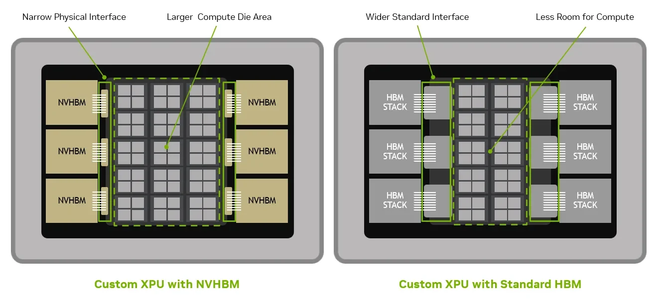
Area savings are achieved primarily through a redesigned physical memory interface (PHY). Standard HBM relies on wider interface connections, increasing the total package footprint. NVHBM uses a custom base die optimized for efficiency, featuring reduced I/O area requirements achieved by moving the memory controller into the 3D HBM stack and integrating a custom PHY.
Compared with the JEDEC HBM4e standard, this design reduces PHY and support area by up to 67%. The narrower interface also simplifies interposer routing, providing up to 80% more usable silicon across the entire layout.
Figure 1. Comparison of die area savings with NVHBM compared to standard HBM
As shown in Figure 1, shrinking the memory interface connections enables the central AI compute die to expand into the newly freed space. This reclamation provides up to a 30% increase in available main-die silicon for compute or other features. The additional silicon area enables XPU designers to add more capabilities within a fixed package footprint.
Power is one of the hardest constraints in modern AI infrastructure. HBM power contributes to the accelerator power budget, package thermal design, rack power envelope, and data center cooling plan. NVHBM enables 15% lower HBM power usage compared to standard HBM4e, creating additional power and thermal headroom for compute.
Power savings matter at multiple levels. At the XPU level, lower HBM power can improve performance per watt and create room for more compute or higher sustained utilization. At the rack level, it can help reduce pressure on power delivery and cooling systems. At AI factory scale, even modest reductions in memory subsystem power can add up across thousands of accelerators. When compounded across an entire 1-gigawatt data center using 2,000W XPUs, power savings can enable up to 15,000 additional XPUs in compute headroom.
The benefit is especially important for large-model inference. XPUs must repeatedly read model weights and KV-cache data while serving users at low latency and high throughput. Reducing the energy spent moving that data can help support faster inference on large models, larger batch sizes, and more efficient use of deployed power.
NVHBM boosts XPU performance and efficiency at the chip level. NVLink Fusion enables hyperscalers and AI natives to connect their XPUs to the rest of the NVIDIA AI platform. By compounding a 30% increase in memory bandwidth, 25% more die area, and 15% HBM power savings, these co-designed architectural improvements translate into a significant 30% overall end-to-end performance increase per XPU.
This connectivity is achieved through the NVLink Fusion chiplet, which bridges custom XPUs and the NVLink fabric, connecting all XPUs in a rack into a single scale-up domain. Now in its sixth generation, NVLink is the only proven, purpose-built scale-up networking fabric for AI factories, delivering leading performance and intelligent resiliency. Upstream, the XPUs can connect to the CPUs via NVLink-C2C.
NVLink Fusion adopters can combine custom XPUs and CPUs with NVIDIA scale-up and scale-out technology stack and ecosystem to reduce development and deployment complexity, increase performance, and accelerate time to market for semi-custom AI factories. And by standardizing on a single unified architecture, NVLink Fusion simplifies operations across the data center, enables flexible reprovisioning of data center capacity, and enables custom AI XPUs to integrate with GPUs for heterogeneous compute.
NVLink Fusion provides a common scale-up foundation for GPUs, custom XPUs and CPUs, networking, and rack-level software. NVHBM complements that foundation with greater memory performance, compute density, HBM power efficiency, and supply resiliency for next-generation accelerators. These technologies give partners a more direct path from custom AI accelerator design to rack-scale deployment and production volume.
Learn more about NVLink Fusion and industry adoption of NVHBM.
The source text above remains the property of its publisher and is reproduced for commentary.